Forks and Branches
The starting point for the new Shruthi synth was to fork from Pichenettes Github.
https://github.com/pichenettes/shruthi-1
A fork is a personal copy of an existing Github project that the developer can do to with whatever you like. A developer can work on their own stuff in their protected bubble and then “push” back up the changes to the original project and thread if the original project wants to incorporate the forked features. A fork is in contrast to a branch, another agile software development term. A branch means a developer takes a copy a project (just like with a fork) with the goal of correcting one or more “issues” or “bugs” that the developer is interested in fixing. By creating the branch everyone on the project is aware of what the developer is trying to fix but they can go off their bubble with the intent that my changes will be compiled and tested solo. Then a kindly wizard associated in the project one day will allow me to “merge” those changes back in to the main Tree of the project.1

So merging gets complicated when we are dealing with files in different electronics CAD packages instead of lines of code. I will use transitioning development software platforms from Eagle (as I will discuss below) to KiCad as an example. If I compared the actual schematic design files on my local hard drive you would be left with a long list of changes of the bits and bytes that no human can use to track changes happened. The file extensions you save into are different the GUI interface is different, none of this can just transfer from one platform to another without a person in the loop. So for this project, I will create a branch and leave breadcrumbs in the Readme.txt file for those curious to work their way back.
After inspecting the original files in the shruthi/hardware_design/pcb folder, I discover these files were originally developed in Eagle 6. The PWB folder contains two types of files .sch and .brd. Currently Eagle is up to version 9.0 and no longer available without bundling together with some other AutoDesk features, which is exactly why the goal is to take these files out of something not exactly maintainable and to move it to Kicad.
Going back to the design folder and searching around this /pwb directory is what I am looking for. These are the schematic and Printed Wiring Board files for multiple designs in the project. 14 designed boards with schematic and PWB design files!
After converting all the schematic files over to inspect them, I found that the original Shruthi product concept isn’t to have fourteen PWB’s on one assembly, but to have the end user select analog boards and plug it into the digital control board, and if the musician wants they can swap between boards for different voices. From the archives, i can see there was an original control board (powered by a micro controller), but at some point the XT version of the Shruthi was released. This version exposed more encoder controls that were hidden behind menus and clicking buttons in lists within the original. For this project it means there may be more pots and buttons to solder, but more fun to mess with when it all works at the end.
I’m going to limit the scope here and after looking back at the build documentation I’m going to start working with two specific boards, the SMR4 mkII_V02. which is a four pole “Roland like” analog filter board, mark II being the second version of this and V02 being the second revision of the second generation.
With these two boards chosen the work begins. Kicad in theory supports Eagle file import but not from the old Eagle files used 12 years ago on the Shruthi2.. So to start, I have to open Eagle to get these Eagle 6 boards rolled up to the newest version and spent a few hours installing this Autodesk Eagle combination, opening the files and then saving them again to be current Eagle files. Once that was completed Kicad successfully recognized the files and could import them.
Kicad and PWB Updates

Now I would just congratulate myself and crack a beer in victory, but I didn’t realize the work had just begun. I had discovered one of the main components for the Analog section of the Synthesizer the LM13700 no longer existed in a PDIP package.
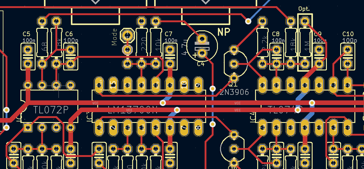
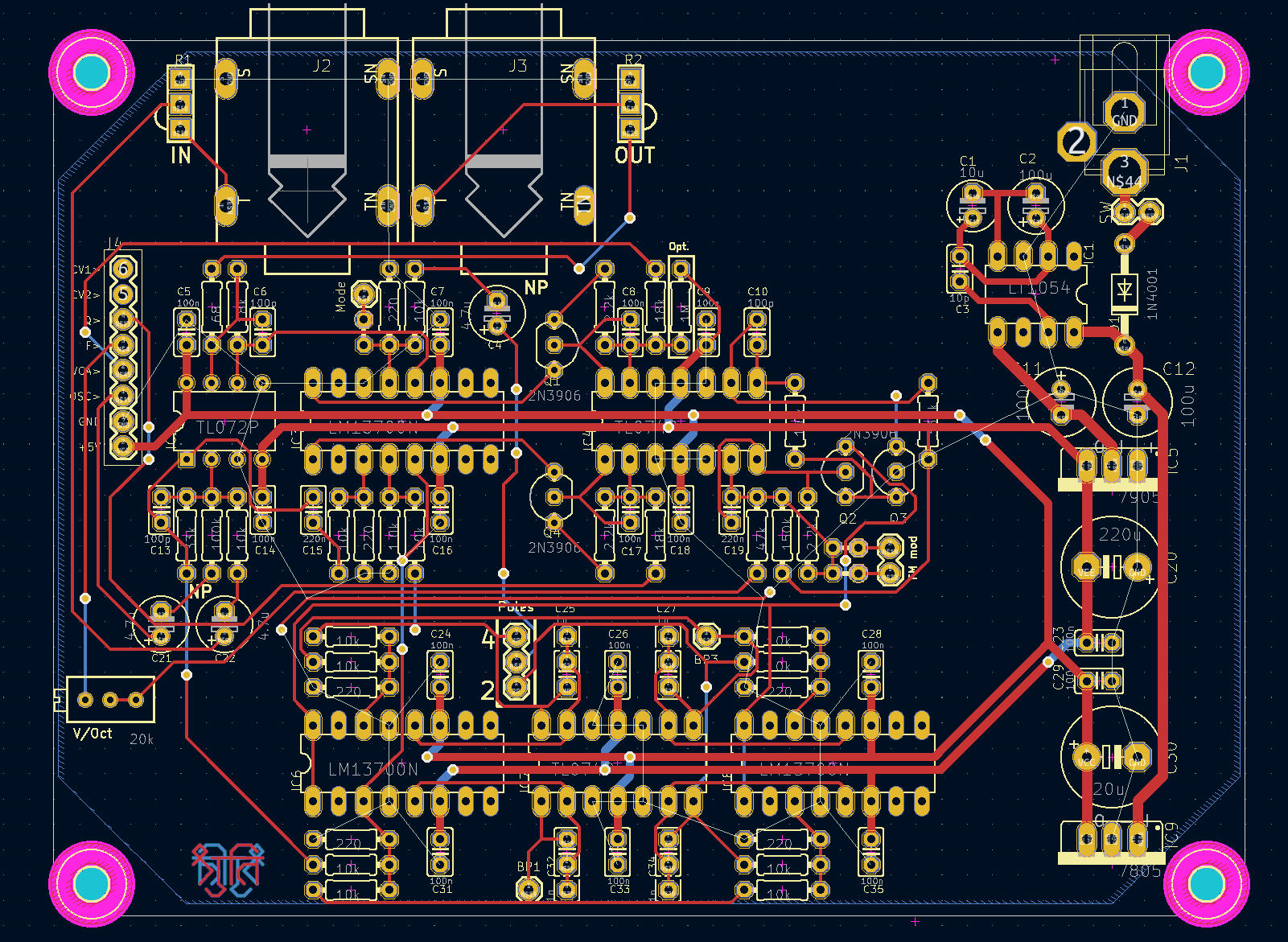
I figured I could solder surface mount (more on that later) and could easily swap out the SOIC version for the PDIP. So I set to work making a new footprint for the part and rewiring the schematic and PWB file to ensure my new part fit. It ended up fitting fine as it was smaller than before but because of the shrinking of the component other assumptions about signal and ground trace lengths had to change and i ended up rerouting more than i planned. I still maintained the two layer setup but much was streamlined and moved from the original SMR_mkII_V02 design to the new SMR_VJK3.
I was lead through the process by the very useful Kicad documentation as well as remembering my old scars using electronics design tools at my day job. Kicad by far was an easier flow than other packages Id used before.

Theory: Transconductance Amplifiers
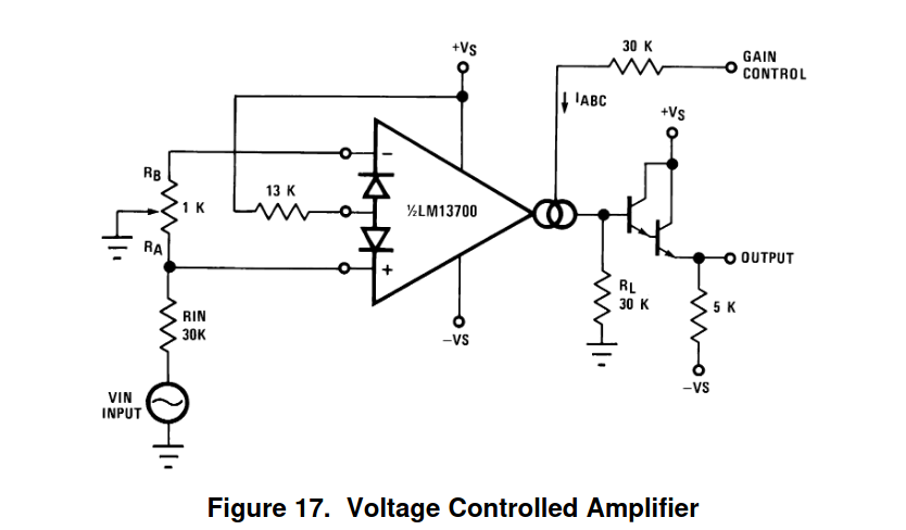
Lets talk about the nitty gritty of the design. So the PWB is quite simple once I got my head around it. It is only a two layer board, with a handful of different through hole parts. Having been the “analog guy” for a few years now the Voltage to current mode transformation of the LM13700 was very interesting. Whats more is that it seems to be a common mode of operation with classic analog synthesizers. Control of the audio signal path is done via potentiometer DC setting the current through these trans conductance amplifiers. This is done both in the gain section of the design as well as the filter section. So the voltage is fixed but the resistance changes and that shifts the level. The diagram below shows an example circuit. So for the gain stage at least its quite obvious that your base current in the output is a function of the gain setting voltage. The current sources used in this application are actually exponential in relationship to the output signal.
And here it is in action within the LPF analog filter board in the Shruthi.
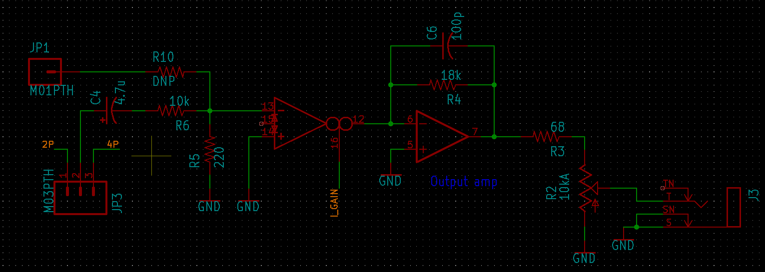
So you can see there’s an off board potentiometer that controls the I_GAIN current and then gets buffered before being driving out the line level cable. I’d love to get deeper into how this is all working (and I Imagine I will in bring-up) but lets get back to the task at hand. The PWB update and removing the PDIP to get an SOIC into the design. Well whacking in the new pads was a piece of cake but since everything got smaller many small changes rippled through the rest of the board.
Back to Board updates
Larger pins mean larger and thicker traces, and once i shrink the pins the room you had is reduced. The thickness of the old device allowed of running voltage rails underneath the part, once i shrunk down to the SOIC i lost all room to do that trick and had to move the rails out from underneath. Now that the power was routed outside, I had to re route the signal traces under or around what Was already there. And finally I noticed a few things i didn’t like so I had to deal with those.
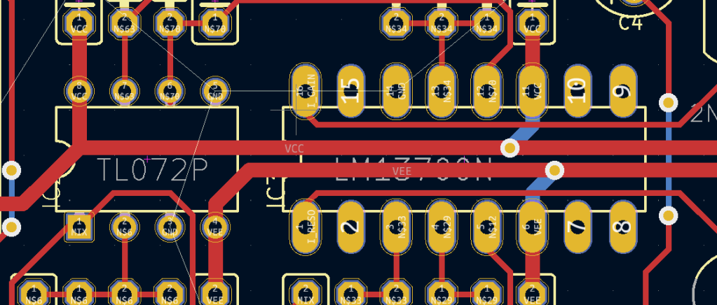

Some other highlights. The DRC settings were set to roughly default but I did space the VDD and VSS on the LM13700’s to be further spaced apart than the older design. My Thought was that the pads also shrunk so any more copper wont move the needle very much. Although we will see in the testing where that ends up.

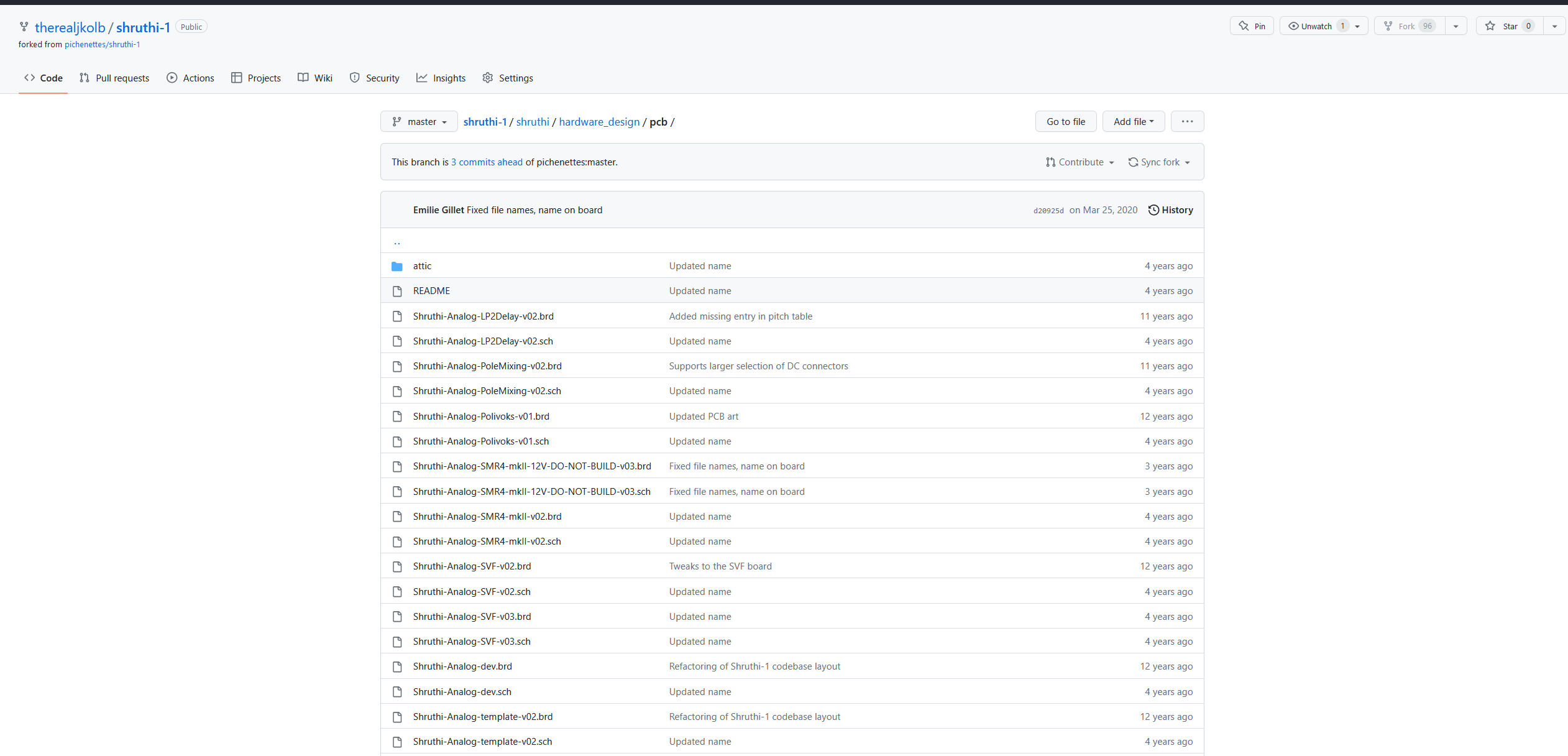
You can take a look at the full design and Kicad files at the project directory for the project.
The next section will be about purchasing the parts for the build as well as an over view of the assembly. The final post will be about testing the end product and lessons learned.
Footnotes
- For more info on forking and how software folks attempt to describe this see https://www.atlassian.com/git/tutorials/comparing-workflows/forking-workflow I decided to fork ultimately after realizing the original project isn’t really active and who knows how far I’ll muck up these original design files.
- Since the time I started this project is now at 7.02 and will probably be further along by the time I post https://www.kicad.org/blog/
- SOIC versus PDIP comparison of footprints.
- Pinchettes does a much better job than me at actually explaining the theory of the VCO/VCF/VCA. At this point im merely an observer until the day I have to debug the thing.
