***Originally written July 2023
After my last post on this project I thought I was losing my mind and all hope was lost. But now I have figured a fundamental boneheaded mistake out and am moving forward again!

I had to address two conflicting theories to resolve this. First, I didn’t trust the custom makefile provided from the repository. I had visions of memory overruns and corruption of some level. I was also suspicions about ESD or mechanical damage of the hardware as I carted this thing back and forth from my lab and my home.
So I soldiered on. The next step I took was to install Microchip Studio and get back to basics. I developed a pure “Blinky” setup to vet the micro itself, without any of the complications of the end application. To be explicit, running Blinky means m to cycle on and off all of the digital output pins and probe them to get a baseline of life. This would remove my concerns about the custom makefile because i was just using the manufacturers IDE.
After toying with Microchip Studio for a while I found that I needed to manually run AVRDUDE to program the .hex file from the command line and hope this would give me the truth I was looking for. I wrote the program to continuously blink all the I/O lines so it would not really give me a blinking LED but it would allow me to probe for life and find any problematic pins. The ATMEGA is setup with various byte accessible ports of I/O (A,B,C,D) that i could write to with a single command.
After getting this new test build loaded I walked through the pins on the micro right at the device with the following results:
| Micro Pin | Good? | Function |
|---|---|---|
| PC7 | Yes | Display Pin 14 (LCD_DATA4) |
| PC6 | Yes | Display Pin 13 (LCD_DATA3) |
| PC5 | No | Display Pin 12 (LCD_DATA_2) |
| PC4 | No | Display Pin 11 (LCD_DATA_1) |
| PC3 | No | Display Pin 6( LCD_EN) |
| PC2 | No | Display pin 4 (LCD_RS) |
| PC1 | Yes | IC1 Pin 5 (SDA) |
| PC0 | Yes | IC1 Pin 6 (SCL) |
| PB7 | Yes | IO_SCK |
| PB6 | Yes | IO_MISO |
| PB5 | Yes | IO_MOSI |
| PB4 | Yes | CV2 |
| PB3 | Yes | CV1 |
| PB2 | Yes | ENC_SW |
| PB1 | Yes | ENC_A |
| PB0 | Yes | ENC_B |
So in my previous few days I was reviewing the differences between the ATMEGA644 as opposed to the newer variant ATMEGA644A. After a few hours of realizing the differences were minimal I threw up my hands in exhaustion. But something stuck in my head. Could the I/Os be used for muliple purposes? And how would JTAG work on this device.
In reviewing the table above I see the pins that don’t work (and coincidentally are connected to my display) are connected to the JTAG interface port. So how does the micro control these different pin modes??
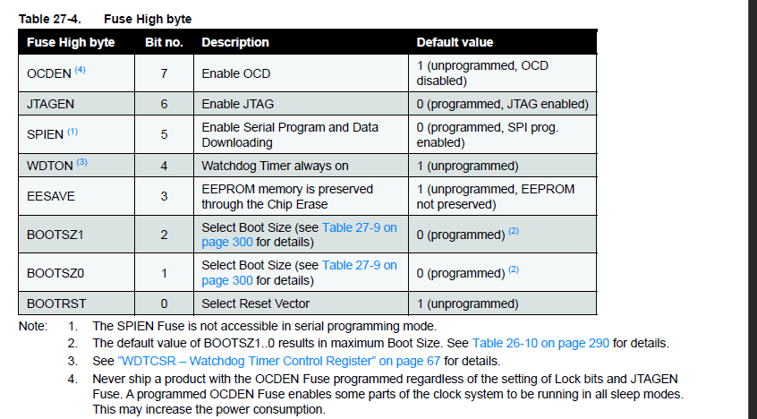
The answer is fuses! I use AVRDUDE to check my high fuse status, and i see that is 0x99! After following the steps on this website.
https://www.instructables.com/How-to-change-fuse-bits-of-AVR-Atmega328p-8bit-mic/
So JTAG is sure enough enabled! I set that JTAGEN bit back to 1 and my clock wave is coming out the pins connected to the display.
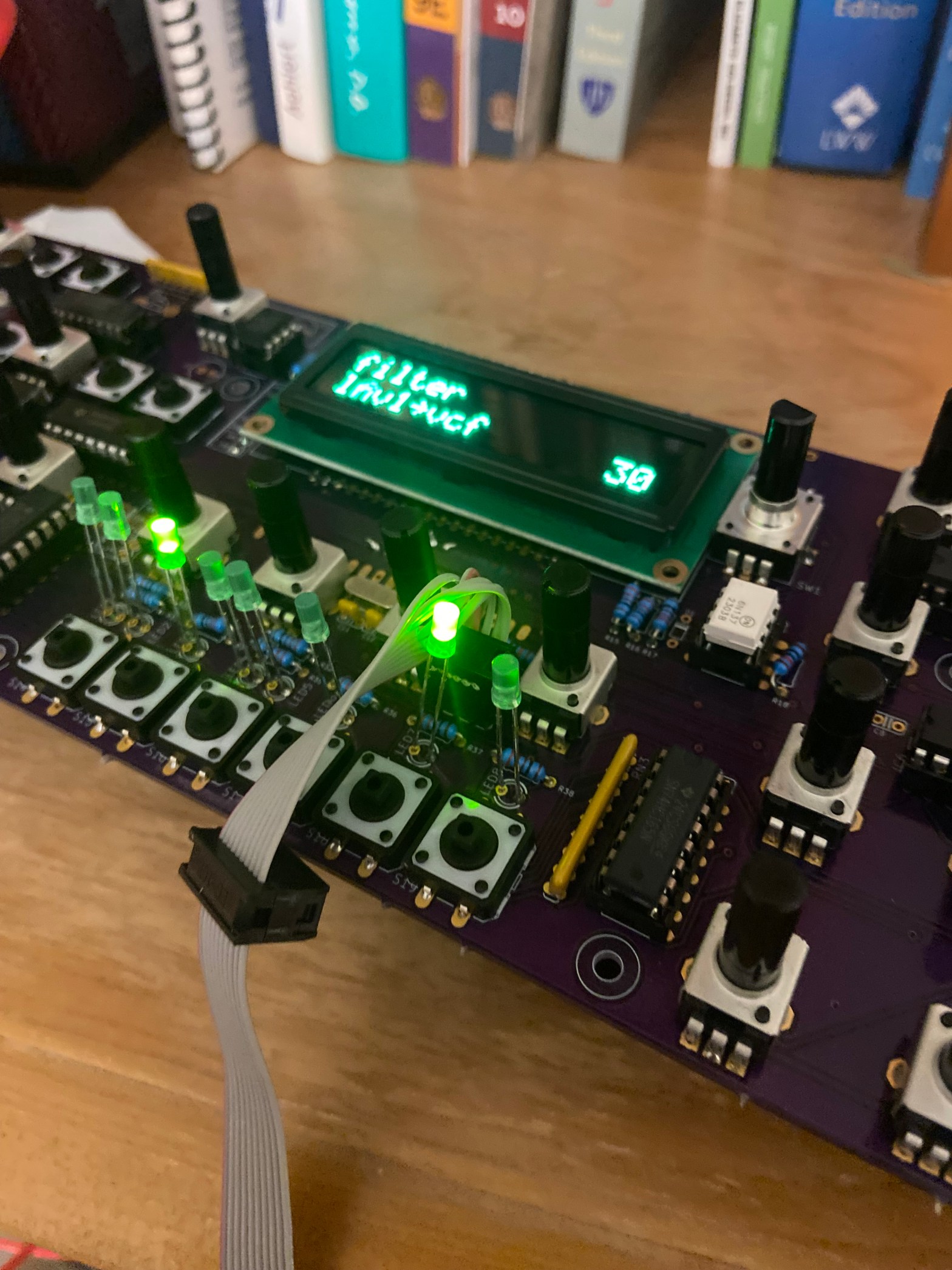
I then proceed to load one of the builds of the the Shruthi source code I made a few months ago and I see activity on the display!!!! WooHoo!
Next Steps
I’m going to setup MIDI stuff now to see what i can control.
A Few Observations
Now I want to reference a few things at this point. The firmware building guide is totally fine for the Shruthi project but it presumes that you have a strong handle on AVR development before starting this modification. So I’ll explain here the gaps
- Clearly pinchettes make and bake commands work
- You need the understanding of memory flash space versus eeprom space versus boot loader space
- You need an understanding of what the AVR fuses mean (here was my tripping point earlier).
