Will put together the final piece that allows us to finally put this project in to the sunset phase.
He confirmed by rolling back the compiler to GCC 4.3.3 (the original compiled version) we could get the unit to actually work as it is supposed to. Apparently, AVR-GCC is available usually through microchip or some various locations and older versions are not available readily. So Will ended up snooping He did it through this GitHub repository (https://github.com/smeshlink/Arduino-Plus/tree/master) a fork of the Arduino main line development from 2013 (11 years ago now!). That repo happened to upload the old AVR-GCC version and will pulled it down and started the compile.
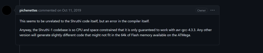
Now, I was warned about this over by the original developer. See the post I read once or twice back when I had all those issues with what ended up being the AVR fuses…
Found wisdom of the comments
I suppose until you have gone down the rabbit hole you don’t really understand what not guaranteed to work really means.
I’ve yet to recompile on my end, but using Will’s compiled build removes all of the chaotic behavior the synthesizer was showing before. One of the points of code that is likely quite dependent on this compiler version is a snippet that occurs in the editor.cc file.
Note that this function does a direct read of program memory via the pgm_read_byte() function. This function is used to directly read pgm memory. In this case, the code works to reading flash out into memory at a specific address as command. Now this could work but the method of using “programmer_switch_mapping + that index means at some point the compiler (no matter how good it is) is not aware of this memory location. The call in this case requires foreknowledge of where this given piece of information resides in active memory. The compiler is unable to check for any sort of error condition in the way it is written. For all it cares, the compiler is presented with a sum of two numbers before passing up to pgm_read_byte. No checks can be done on whether the memory is valid or not or if there is anything at the target address.
I can imagine something like this was done to same memory usage in a constrained design (to do: is there a linker output report?) if you aren’t going to use up these things as much in the code space. But again this is mere speculation. At least at the moment we have functioning products.
New PWBs and manufacturing errors
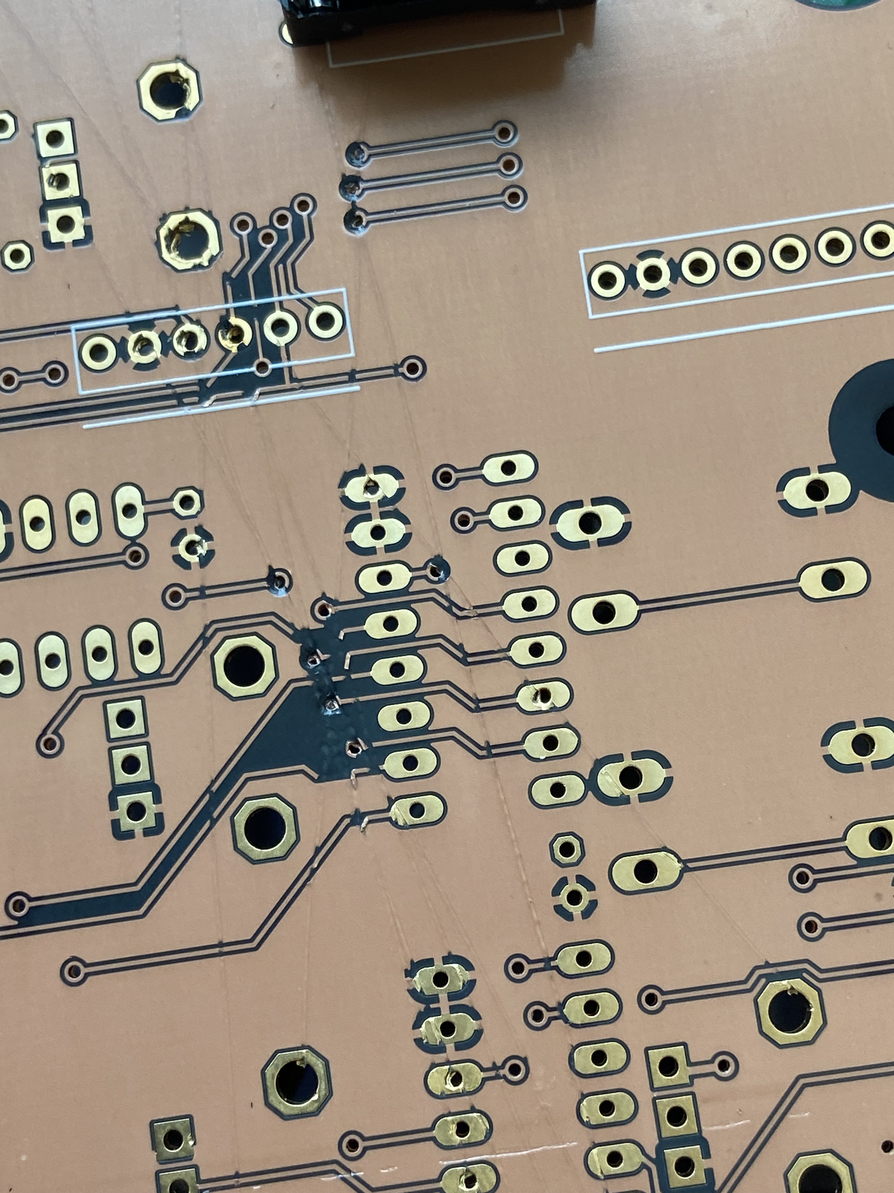
I received a new set of PWBS this week. I was excited to build and started soldering them up when I saw this
Note those cuts in the PWB
Traces broken in multiple sections of the board from what looks like a razor blade or something run across the board. Whats odd is its just one out of the group of boards so I didn’t lose my entire $230 on these from OSH park. I emailed them out and received a very quick response. They let me know this board should have been screened out of my order as a test sample and I’ve gotten the extra boards as a show of good faith.
I do like the aesthetic of the clear solder mask style, but with so much of the copper plane covering each side I think I’ve lost the cool factor that would have come with more black.
“It’s possible the fab was attempting to indicate an etching failure on that one copy. During AOI testing they’ll scratch the traces, which lets someone else down the line know to mark it with a big silver “X” so we can notice it and get a replacement started. “
Onward to soldering up this round of boards and getting prototypes out to my friends. Will is still on the enclosure part then we can start packing this project up.
Roadmap
Build the remainder of analog and digital units
Send them to friends!
Design and fab cases for these synths
Create a lessons learned
Random Observations
Until this point my head was so deep in the design I never questioned the original name of this synth the Shruthi. I happened to mis type a google search and I learned that this is an accordion like drone instrument out of India. Some links below.
https://gcc.gnu.org/releases.html I’m not quite sure about my AVR-GCC comments any more or even whether or not AVR-GCC is just standard GCC wrapped with some libraries. I have gotten turned around on this on. Something to report back on in another post.
After my last post on this project I thought I was losing my mind and all hope was lost. But now I have figured a fundamental boneheaded mistake out and am moving forward again!
There is life!
I had to address two conflicting theories to resolve this. First, I didn’t trust the custom makefile provided from the repository. I had visions of memory overruns and corruption of some level. I was also suspicions about ESD or mechanical damage of the hardware as I carted this thing back and forth from my lab and my home.
So I soldiered on. The next step I took was to install Microchip Studio and get back to basics. I developed a pure “Blinky” setup to vet the micro itself, without any of the complications of the end application. To be explicit, running Blinky means m to cycle on and off all of the digital output pins and probe them to get a baseline of life. This would remove my concerns about the custom makefile because i was just using the manufacturers IDE.
After toying with Microchip Studio for a while I found that I needed to manually run AVRDUDE to program the .hex file from the command line and hope this would give me the truth I was looking for. I wrote the program to continuously blink all the I/O lines so it would not really give me a blinking LED but it would allow me to probe for life and find any problematic pins. The ATMEGA is setup with various byte accessible ports of I/O (A,B,C,D) that i could write to with a single command.
After getting this new test build loaded I walked through the pins on the micro right at the device with the following results:
Micro Pin
Good?
Function
PC7
Yes
Display Pin 14 (LCD_DATA4)
PC6
Yes
Display Pin 13 (LCD_DATA3)
PC5
No
Display Pin 12 (LCD_DATA_2)
PC4
No
Display Pin 11 (LCD_DATA_1)
PC3
No
Display Pin 6( LCD_EN)
PC2
No
Display pin 4 (LCD_RS)
PC1
Yes
IC1 Pin 5 (SDA)
PC0
Yes
IC1 Pin 6 (SCL)
PB7
Yes
IO_SCK
PB6
Yes
IO_MISO
PB5
Yes
IO_MOSI
PB4
Yes
CV2
PB3
Yes
CV1
PB2
Yes
ENC_SW
PB1
Yes
ENC_A
PB0
Yes
ENC_B
So in my previous few days I was reviewing the differences between the ATMEGA644 as opposed to the newer variant ATMEGA644A. After a few hours of realizing the differences were minimal I threw up my hands in exhaustion. But something stuck in my head. Could the I/Os be used for muliple purposes? And how would JTAG work on this device.
In reviewing the table above I see the pins that don’t work (and coincidentally are connected to my display) are connected to the JTAG interface port. So how does the micro control these different pin modes??
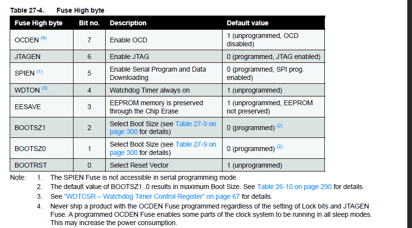
Excerpt from ATMEGA644A datasheet
The answer is fuses! I use AVRDUDE to check my high fuse status, and i see that is 0x99! After following the steps on this website.
So JTAG is sure enough enabled! I set that JTAGEN bit back to 1 and my clock wave is coming out the pins connected to the display.
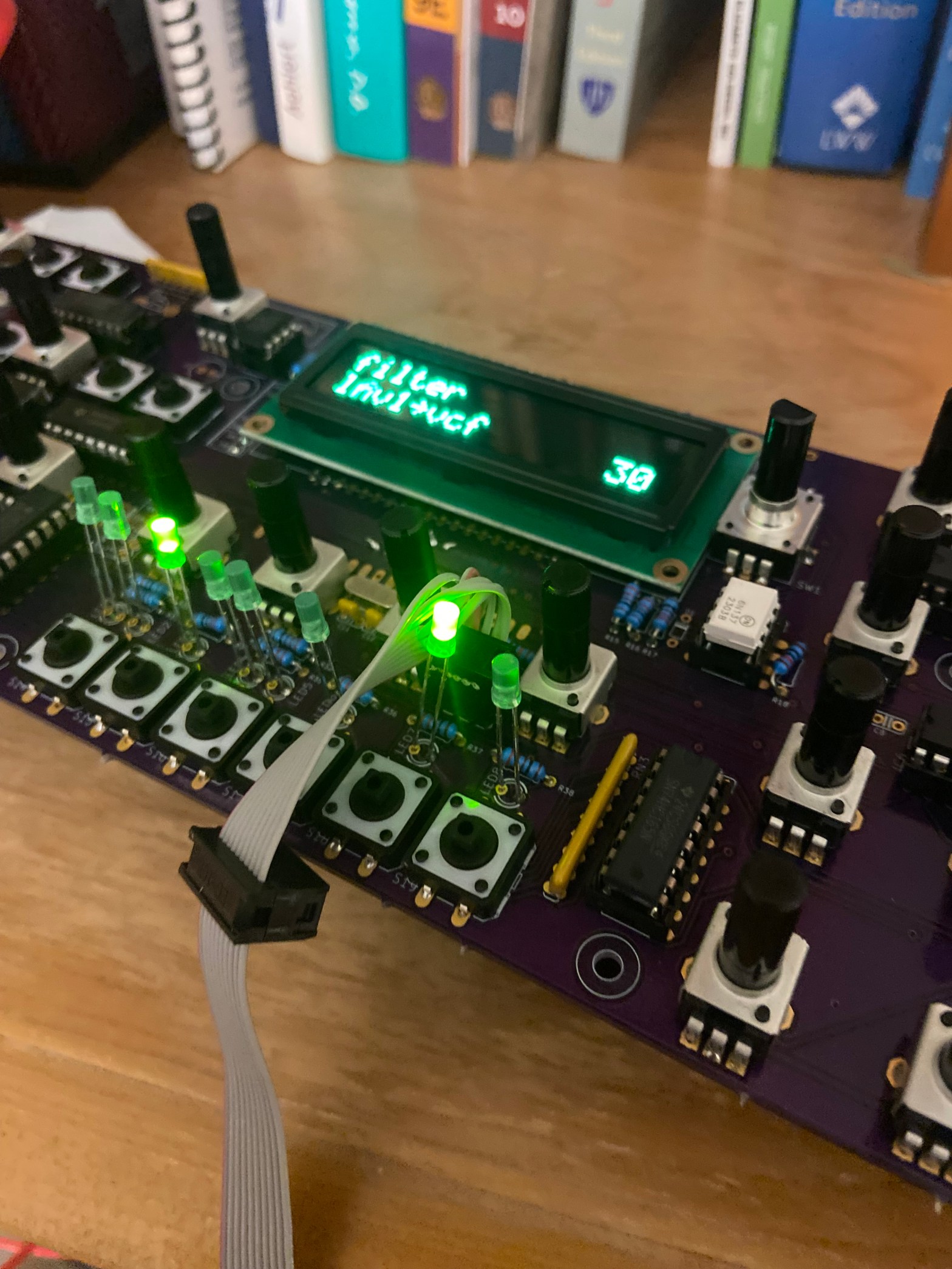
I then proceed to load one of the builds of the the Shruthi source code I made a few months ago and I see activity on the display!!!! WooHoo!
Next Steps
I’m going to setup MIDI stuff now to see what i can control.
A Few Observations
Now I want to reference a few things at this point. The firmware building guide is totally fine for the Shruthi project but it presumes that you have a strong handle on AVR development before starting this modification. So I’ll explain here the gaps
Clearly pinchettes make and bake commands work
You need the understanding of memory flash space versus eeprom space versus boot loader space
You need an understanding of what the AVR fuses mean (here was my tripping point earlier).
A fork is a personal copy of an existing Github project that the developer can do to with whatever you like. A developer can work on their own stuff in their protected bubble and then “push” back up the changes to the original project and thread if the original project wants to incorporate the forked features. A fork is in contrast to a branch, another agile software development term. A branch means a developer takes a copy a project (just like with a fork) with the goal of correcting one or more “issues” or “bugs” that the developer is interested in fixing. By creating the branch everyone on the project is aware of what the developer is trying to fix but they can go off their bubble with the intent that my changes will be compiled and tested solo. Then a kindly wizard associated in the project one day will allow me to “merge” those changes back in to the main Tree of the project.1
A good infograhic from theserverside.com
So merging gets complicated when we are dealing with files in different electronics CAD packages instead of lines of code. I will use transitioning development software platforms from Eagle (as I will discuss below) to KiCad as an example. If I compared the actual schematic design files on my local hard drive you would be left with a long list of changes of the bits and bytes that no human can use to track changes happened. The file extensions you save into are different the GUI interface is different, none of this can just transfer from one platform to another without a person in the loop. So for this project, I will create a branch and leave breadcrumbs in the Readme.txt file for those curious to work their way back.
After inspecting the original files in the shruthi/hardware_design/pcb folder, I discover these files were originally developed in Eagle 6. The PWB folder contains two types of files .sch and .brd. Currently Eagle is up to version 9.0 and no longer available without bundling together with some other AutoDesk features, which is exactly why the goal is to take these files out of something not exactly maintainable and to move it to Kicad.
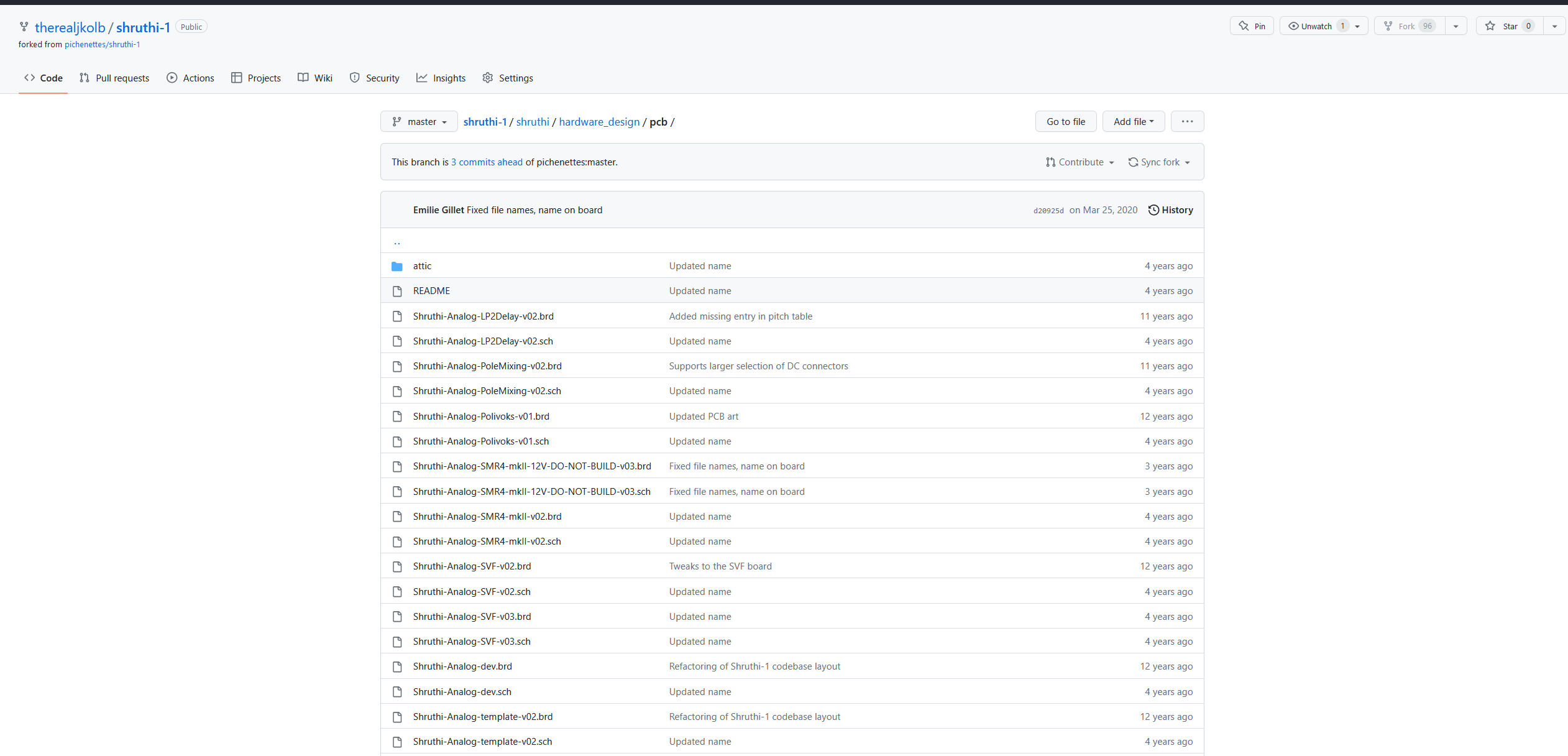
Going back to the design folder and searching around this /pwb directory is what I am looking for. These are the schematic and Printed Wiring Board files for multiple designs in the project. 14 designed boards with schematic and PWB design files!
The Github Shruthi PWB directory
After converting all the schematic files over to inspect them, I found that the original Shruthi product concept isn’t to have fourteen PWB’s on one assembly, but to have the end user select analog boards and plug it into the digital control board, and if the musician wants they can swap between boards for different voices. From the archives, i can see there was an original control board (powered by a micro controller), but at some point theXT versionof the Shruthi was released. This version exposed more encoder controls that were hidden behind menus and clicking buttons in lists within the original. For this project it means there may be more pots and buttons to solder, but more fun to mess with when it all works at the end.
I’m going to limit the scope here and after looking back at thebuild documentation I’m going to start working with two specific boards, the SMR4 mkII_V02. which is a four pole “Roland like” analog filter board, mark II being the second version of this and V02 being the second revision of the second generation.
With these two boards chosen the work begins. Kicad in theory supports Eagle file import but not from the old Eagle files used 12 years ago on the Shruthi2.. So to start, I have to open Eagle to get these Eagle 6 boards rolled up to the newest version and spent a few hours installing this Autodesk Eagle combination, opening the files and then saving them again to be current Eagle files. Once that was completed Kicad successfully recognized the files and could import them.
Kicad and PWB Updates
Kicad Up and Running with the Converted Board File
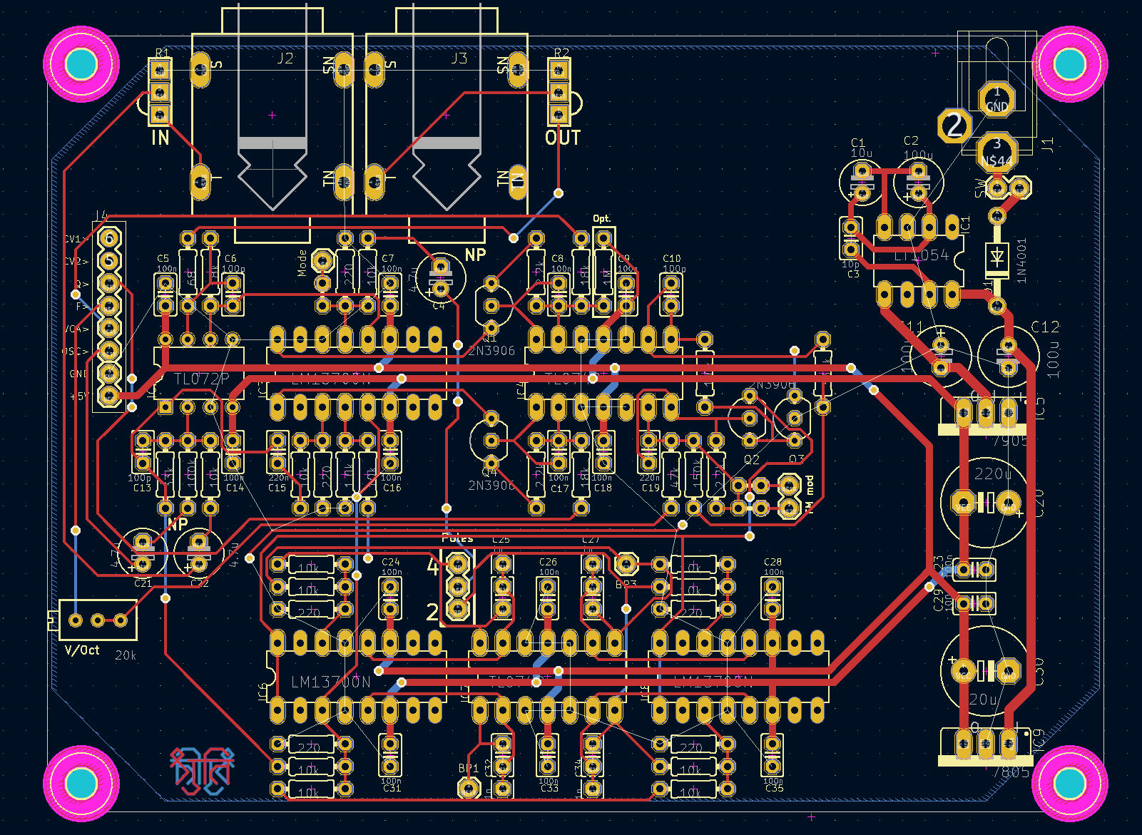
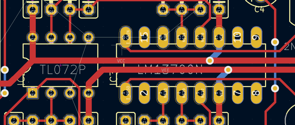
Now I would just congratulate myself and crack a beer in victory, but I didn’t realize the work had just begun. I had discovered one of the main components for the Analog section of the Synthesizer the LM13700 no longer existed in a PDIP package.
I figured I could solder surface mount (more on that later) and could easily swap out the SOIC version for the PDIP. So I set to work making a new footprint for the part and rewiring the schematic and PWB file to ensure my new part fit. It ended up fitting fine as it was smaller than before but because of the shrinking of the component other assumptions about signal and ground trace lengths had to change and i ended up rerouting more than i planned. I still maintained the two layer setup but much was streamlined and moved from the original SMR_mkII_V02 design to the new SMR_VJK3.
I was lead through the process by the very useful Kicad documentation as well as remembering my old scars using electronics design tools at my day job. Kicad by far was an easier flow than other packages Id used before.
Imported Original Analog Filter BoardImported Original Schematic
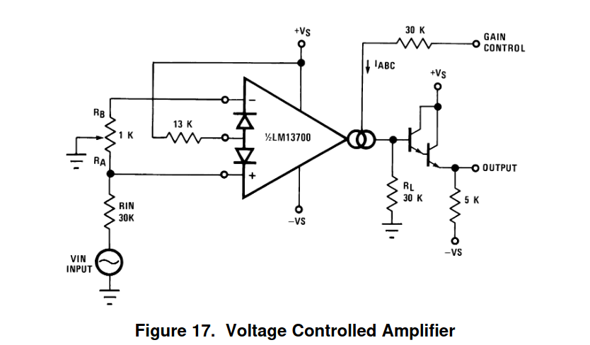
Theory: Transconductance Amplifiers
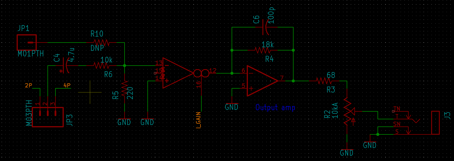
Lets talk about the nitty gritty of the design. So the PWB is quite simple once I got my head around it. It is only a two layer board, with a handful of different through hole parts. Having been the “analog guy” for a few years now the Voltage to current mode transformation of the LM13700 was very interesting. Whats more is that it seems to be a common mode of operation with classic analog synthesizers. Control of the audio signal path is done via potentiometer DC setting the current through these trans conductance amplifiers. This is done both in the gain section of the design as well as the filter section. So the voltage is fixed but the resistance changes and that shifts the level. The diagram below shows an example circuit. So for the gain stage at least its quite obvious that your base current in the output is a function of the gain setting voltage. The current sources used in this application are actually exponential in relationship to the output signal.
LM13700 Example Circuit
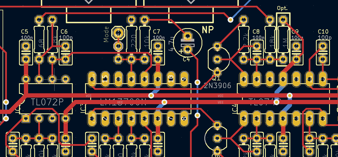
And here it is in action within the LPF analog filter board in the Shruthi.
Note the Amplifier with the two large circles
So you can see there’s an off board potentiometer that controls the I_GAIN current and then gets buffered before being driving out the line level cable. I’d love to get deeper into how this is all working (and I Imagine I will in bring-up) but lets get back to the task at hand. The PWB update and removing the PDIP to get an SOIC into the design. Well whacking in the new pads was a piece of cake but since everything got smaller many small changes rippled through the rest of the board.
Back to Board updates
Larger pins mean larger and thicker traces, and once i shrink the pins the room you had is reduced. The thickness of the old device allowed of running voltage rails underneath the part, once i shrunk down to the SOIC i lost all room to do that trick and had to move the rails out from underneath. Now that the power was routed outside, I had to re route the signal traces under or around what Was already there. And finally I noticed a few things i didn’t like so I had to deal with those.
Original Layout of DIP LM13700NNew Layout of the Same Section.
Some other highlights. The DRC settings were set to roughly default but I did space the VDD and VSS on the LM13700’s to be further spaced apart than the older design. My Thought was that the pads also shrunk so any more copper wont move the needle very much. Although we will see in the testing where that ends up.
Overview of the New PWB design
You can take a look at the full design and Kicad files at the project directory for the project.
The next section will be about purchasing the parts for the build as well as an over view of the assembly. The final post will be about testing the end product and lessons learned.
Since the time I started this project is now at 7.02 and will probably be further along by the time I post https://www.kicad.org/blog/
SOIC versus PDIP comparison of footprints.
Pinchettes does a much better job than me at actually explaining the theory of the VCO/VCF/VCA. At this point im merely an observer until the day I have to debug the thing.